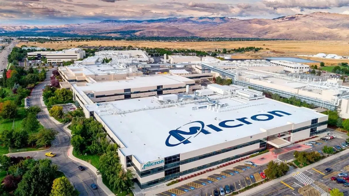
Micron Technology has started the operations of its state of art semiconductor plant at Sanand, Gujarat, with the largest raised floor clean room in the world of 500,000 sq ft.
The plant was inaugurated on February 28, 2026, by Prime Minister Narendra Modi to mark the beginning of the era of sophisticated memory manufacturing in India when the first DRAM modules were shipped to Dell Technologies.
What are the Clean Room Engineering Capabilities?
The clean room is rated Class 1000 and particles are restricted to less than 1,000 per cubic meter with 120 times per hour air recirculated, which is a far greater rate than the norms in the pharmaceutical industry, to guard nanoscale particles.
It was designed to withstand the moisture and soil of Gujarat, and the gold bonding wires used in creating the product are smaller than a human hair. This one-level wonder is the largest globally, which allows processing in large quantities.
Production Processes of Memory
The ATMP (Assembly, Testing, Marking, Packaging) facility deals with DRAM - volatile working memory of computers, smartphones, and data centers - and NAND flash of non-volatile storage in SSDs.
Micron international fabs process wafers which are then subjected to thinning, dicing, assembly, intense testing and packaging of modules which are either exported or domestically supplied. First product sales are to partners such as Dell, Asus, and Qualcomm, and tens of millions of ICs in 2026 would be to almost one billion in 2027.
Investment and Gradual Growth
The total investment is composed of 2 stages of investment of $2.7 billion and is supported by the incentives of Semiconductor Mission by India (50 percent of the fiscal incentive) and Gujarat (20 percent).
Phase 1 centers on ramped-up with the facility becoming a key location in the global network of Micron together with the fabs in the US, Taiwan, and Singapore.
The plant hired 1,300 employees, half of whom are fresh Gujarat engineers, with a university curriculum designed to suit its requirements and then they were sent to 3-6 months of training in Malaysia and Singapore.
The automation of AI, yield, and factory intelligence ensures the efficiency of the world level, developing the local competence in the conditions of the global lack of talents.
The Semiconductor Mission in India
Later rolled out in 2021, the mission has been greenlit by several units, such as Tata with its Dholera fab and OSAT facilities nearby, to reduce the 95% of all imported chips to India and create 20,000 jobs ecosystem-wide.
Gujarat Sanand is a center that will complement automotive giants and attract ancillaries.
In this venture, AI, EVs, and 5G supply chain resilience is enhanced and exports lead to forex savings. It also goes with Make in India and improves the national security on the essential tech when the US and China are on heightened tensions. Issues such as the long-term talent pipelines persistence are still there, and the success of the clean room is a standard that will be followed in other fabs.


Comments
All Comments (0)
Join the conversation